Table of Contents

Table of Contents
Wiley-SID Series in Display Technology

Copyright © 2012 by John Wiley & Sons, Inc. All rights reserved.
Published by John Wiley & Sons, Inc., Hoboken, New Jersey.
Published simultaneously in Canada.
No part of this publication may be reproduced, stored in a retrieval system, or transmitted in any form or by any means, electronic, mechanical, photocopying, recording, scanning, or otherwise, except as permitted under Section 107 or 108 of the 1976 United States Copyright Act, without either the prior written permission of the Publisher, or authorization through payment of the appropriate per-copy fee to the Copyright Clearance Center, Inc., 222 Rosewood Drive, Danvers, MA 01923, (978) 750-8400, fax (978) 750-4470, or on the web at . Requests to the Publisher for permission should be addressed to the Permissions Department, John Wiley & Sons, Inc., 111 River Street, Hoboken, NJ 07030, (201) 748-6011, fax (201) 748-6008, or online at .
Limit of Liability/Disclaimer of Warranty: While the publisher and author have used their best efforts in preparing this book, they make no representations or warranties with respect to the accuracy or completeness of the contents of this book and specifically disclaim any implied warranties of merchantability or fitness for a particular purpose. No warranty may be created or extended by sales representatives or written sales materials. The advice and strategies contained herein may not be suitable for your situation. You should consult with a professional where appropriate. Neither the publisher nor author shall be liable for any loss of profit or any other commercial damages, including but not limited to special, incidental, consequential, or other damages.
For general information on our other products and services or for technical support, please contact our Customer Care Department within the United States at (800) 762-2974, outside the United States at (317) 572-3993 or fax (317) 572-4002.
Wiley also publishes its books in a variety of electronic formats. Some content that appears in print may not be available in electronic formats. For more information about Wiley products, visit our web site at .
Library of Congress Cataloging-in-Publication Data
Tsujimura, Takatoshi.
OLED displays: fundamentals and applications / Takatoshi Tsujimura.
p. cm.
Includes bibliographical references and index.
ISBN 978-1-118-14051-2
1. Flat panel displays. 2. Electroluminescent devices. 3. Organic semiconductors. I. Title.
TK7882.I6T83 2011
621.3815'422–dc23
2011027371
Series Editor’s Foreword
I have long aspired to publish a book on OLED technology in this series. From the beginning, the problem I encountered was that the technology was so new and was developing so rapidly that any book written would have been out of date before it was published. Although the technology is still developing at a prodigious rate, it has reached a level of maturity that at last makes possible the publication of a book covering all aspects of OLED technology from a fundamental description of light emission from OLED materials through TFT design to manufacturing techniques and applications not just to displays but also to lighting. Books previously published in the field have essentially been collections of research papers. Useful as such books are, they do not fulfill the objectives of the Wiley-SID series, so I hope that those who require a text covering all aspects of this important technology will consider this latest book in the series to have been well worth the wait.
To provide the reader with a précis of the scope of this book, after an introductory chapter which focuses on early OLED-based products, Chapter 2 contains a brief history of OLED development and then goes on to describe in detail and on the basis of actual device structures the electronic and thermodynamic fundamentals of light emission from small molecule and polymeric, singlet and triplet OLED materials, the mechanisms of charge injection, transfer and recombination, electron and optical efficiency, and degradation and lifetime issues. This chapter contains all of the science of the operation of a light-emitting OLED structure.
Chapter 3 describes the manufacturing processes for all of the layers in a working OLED device and covers purification and deposition processes, monitoring techniques for quality control, defects and degradation phenomena, and the methods for their detection and analysis. Chapter 4 describes what is required to convert OLED devices into actual display modules which can use either active or passive matrix addressing. Chapter 5 discusses TFT addressing circuitry based on LTPS technology and describes in detail the specific requirements for the circuit designs required by current-driven OLED technology. Chapter 6 addresses the next generation of OLED technology, and covers patterning techniques, solution processed materials, new higher yield manufacturing processes, and improved TFT technologies. The book concludes with chapters on OLED lighting and on new display applications of OLEDs in large size and flexible displays.
Dr. Tsujimura has been actively involved in OLED display development since the early days in the 1990s when active matrix TFT technology reached a stage of development that made high pixel count OLED displays technologically feasible. His expertise in the technology is both deep and broad, as readers will appreciate when they delve deeper into this latest addition to the series.
Anthony C. Lowe
Series Editor
Braishfield, United Kingdom
Preface
Organic light-emitting diode (OLED) and liquid crystal display (LCD) technologies are often compared side by side; however, the LCD is the successful predecessor of the OLED display. According to the experience of this author, who was engaged in developing LCD displays from phase 1 thin-film transistor (TFT) LCD line manufacturing in the past, it is somewhat miraculous that the relatively new OLED and the well-established, mature LCD technologies are compared on an apples-to-apples basis or as parallel technologies. This comparison indicates the inherently high quality of OLED displays.
The success of the vast market for LCD displays can be attributed not only to the intensive research and development efforts of the display manufacturers proper (Samsung, Sharp, LG Display, etc.) but also to the contributions of various individuals involved in components and equipment testing, measurement, and manufacturing, and in both marketing and academic research. The author hopes that the OLED industry will benefit from equally vigorous and numerous contributions of specialists either directly or indirectly involved in OLED manufacturing, and that the OLED market will eventually become as wide and robust as the LCD market is today.
The LCD industry grew in tandem with developments in related fields (manufacturing equipment testing, etc.); thus there are many aspects applicable to OLED technology, which are discussed in detail in this book. Each topic is presented with a discussion of its basic theory and background, followed by description and examples of its practical application. The author has tried to present all of these technologies in as broad a scope as possible to ensure that readers involved in all aspects of OLED research and development will benefit from this book.
On receiving the SID Special Recognition award in 2007, the author expressed his desire to make significant contributions to, and thus fortify and expand the fledgling OLED industry. The author hopes that this book will help in achieving that objective, and that it will contribute to the overall industrywide growth of OLED technology.
Takatoshi Tsujimura
1
Introduction
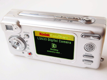
The basic structure of organic light-emitting diodes (OLEDs) was reported by Ching W. Tang and Steven Van Slyke at Eastman Kodak in 1987 [1]. This was a groundbreaking study and was later referred to as the “first OLED paper.” Now, almost 25 years later, there is a large market place for OLED devices. After the first active-matrix-driven OLED (AMOLED) display was introduced by SK Display (a joint manufacturing venture by Eastman Kodak and Sanyo Electric), the first product using an AMOLED display was Kodak’s LS633 digital camera (see ). This was followed by the widescale development of many other OLED-based products, including cellular phones, audioplayers (), portable multimedia players (), and portable global positioning satellite (GPS) devices, which now provide high-resolution displays in brilliant, multitone colors.
The first active-matrix OLED display product on the market (Kodak LS633 digital camera).
Example of an audioplayer using active-matrix OLED (AMOLED) (Sony Walkman NW-X-1050).

Example of a personal multimedia player using AMOLED (Dynaconnective Dawin; original equipment manufacturer [OEM] product of the Neosol Cliod).

Larger-display products have also been introduced on the market, such as those shown in Figs. and . Much larger (e.g., 20–400-in.) prototypes have also been developed. Because of superior features such as slim flatscreen design and aesthetically pleasing screen image, and due to high-contrast image signal emission and very good response time, the current state of the art of OLED television technology that has debuted in the marketplace is indeed unprecedented. [2]
Digital photo frame obtained using 8-in. OLED screen (Kodak OLED wireless frame).

An 11-in.-screen television set (Sony XEL-1).

The main objective of this book is to explain the basics and application of this promising technology from various perspectives.
References
1. C. W. Tang and S. A. Van Slyke, Organic electroluminescent diodes, Appl. Phys. Lett. 51(12):913–915 (1987).
2. T. Tsujimura, W. Zhu, S. Mizukoshi, N. Mori, M. Yamaguchi, K. Miwa, S. Ono, Y. Maekawa, K. Kawabe, M. Kohno, and K. Onomura, Advancements and outlook of high performance active-matrix OLED displays, SID 2007 Digest, 2007, p. 84.
2
OLED Display Structure
Before any in-depth discussion of OLED display structure, let us consider the initial origins of OLED technology, which are based on early observations of electroluminescence. In the early 1950s, a group of investigators at Nancy University in France applied high-voltage alternating-current (AC) fields in air to acridine orange and quinacrine, which were dissolved in or deposited on thin-film cellulose or cellophane [1]. One mechanism identified in these processes involved excitation of electrons. Then in 1960 a team of investigators at New York University (NYU) made ohmic dark-injecting electrode contacts to organic crystals and described the necessary workfunctions (energy requirements) for hole and electron-injecting electrode contacts [2]. These contacts are the source of charge injection in all present-day OLED devices. The same NYU group also studied direct-current (DC) electroluminescence (EL) in vacuo on a single pure anthracene crystal and tetracene-doped anthracene crystals in the presence of a small-area silver electrode at 400 V [3]. The proposed mechanism for this reaction was termed field-accelerated electron excitation of molecular fluorescence. The NYU group later observed that in the absence of an external electric field, the EL in anthracene crystals results from recombination of electron and hole, and that the conducting-level energy of anthracene is higher than the exciton energy level [4].
Because of the association between electroluminescence and later OLED development on the basis of these and other early EL studies, the term organic EL gradually emerged and is still used today. Electroluminescence includes two basic phenomena:
Phenomenon 1 is the narrower definition. Current OLED devices, after Tang and Van Slyke’s “first OLED paper,” utilize LED-like emission mechanisms, that is, phenomenon 2.
Table lists the differences between a liquid crystal display (LCD) and an OLED display. The OLED has a very short response time and is capable of using “punching” (an imaging technique for enhancing the local luminance to emphasize the highlighted region of an image). The punching technique is used in cathode ray tubes (CRTs), which can have much higher luminance of a dot than the screen luminance. An OLED can use a similar operation, while a normal LCD display cannot.
Differences between Liquid Crystal and OLED Displays
| Parameter | LCD | OLED |
| Response time | Slow; hold-like (delayed) | Fast, impulse-like (rapid) |
| Punching | Difficult | Possible
 |
| Viewing angle | Narrower high contrast angle region | Lambertian distribution |
| Number of components | More | Fewer |
| Differential aging | Small | Larger |
| Susceptibility to water and O2 | Small | Larger |
Outgoing light distribution whose luminace is proportional to cosθ.
Luminance reduction in terms of use of a particular pixel and between colors.
Table outlines the chronological history of OLED technology development. This table was prepared by the Society for Information Display (SID), which holds the world’s largest conference on this topic.
Timeline for OLED Technology Development
Source: SID International Symposium (2003), 40 Years of SID Symposia—Nurturing Progress in EL/OLED Technology, Baltimore, MD.
| Year | Event | Company/Institute |
| 1960–mid–1970s | D OLED crystal molecule, anthracene, etc. | NRC (Canada), RCA |
| 1987 | P OLED diode structure paper in Appl. Phys. Lett. | Eastman Kodak |
| 1990 | P first PLED paper in Nature | Cambridge Univ. |
| 1996 | P first AMOLED demonstration (QVGA) | TDK |
| 1998 | D first phosphorescence OLED | Princeton Univ. |
| 1999 | D first passive OLED product | Pioneer |
| 2001 | D 0.72-in. headmount display by AMOLED on silicon | eMagin |
| 2001 | D 13-in. SVGA AMOLED prototype | Sony |
| 2001 | D 2.1-in. 130-ppi AMOLED prototype | Seiko Epson/CDT |
| 2002 | D 15-in. 1280 × 720 OLED prototype | Eastman Kodak/Sanyo |
| 2003 | D digital camera with 2.2-in. AMOLED display | Eastman Kodak |
| 2003 | D Tiled 24-in. AMOLED prototype with by 12-in. display | Sony |
| 2003 | D 20-in. phosphorescence AMOLED prototype by a-Si backplane | ChiMei/IDT/IBM |
Abbreviations in this column: a-si—amorphous silicon; AMOLED—active-matrix OLED; D—development of; P—publication or presentation/demonstration of; PLED—polymer (O)LED; ppi—pixels per inch; QVGA—quarter videographics array (320 × 240 pixels); SVGA—super videographics array (800 × 600 pixels).
The chronological sequence of development listed in reflects the emergence of some general form of classification of OLED technologies, including
The developments listed here and in indicate that the rapid advances in OLED technologies resulted from extensive experimental trial and error. Each technology is discussed in further detail later in the book.
Emission from all OLED devices—whether of the small-molecular or polymer family—can be explained by the same principle. Through electron–hole recombination, a high-energy molecular state is formed. This state is called an exciton, as it behaves like a single molecule with high energy. This exciton generates light after an exciton lifetime period (). [Another type of emission, termed photoluminescence (PL) emission, is caused by light (e.g., UV)-induced molecular excitation.]
Diagram of the OLED emission mechanism.
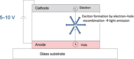
The wavelength of this light emission corresponds to the exciton energy, so it is possible to control the color of the emission by adjusting the molecular design of the color center. This feature is quite advantageous for OLED display applications.
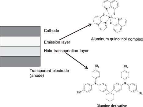
In experimentation using tetracene-doped anthracene crystals and materials, OLED emission had been observed before the so-called first OLED paper in 1987 [5] (see Row 1 in [6]). However, the voltage and efficiency levels were insufficient for actual application. The scenario depicted in and described in the Tang–Van Slyke paper [5] represents advanced concepts that remain valid today:
OLED device reported by Tang and Van Slyke in 1987 [5].
OLED devices could emit very dim light before these developments, but high-luminance operation was achieved only after the first OLED paper.
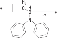
As mentioned earlier, the two basic families of OLED are small-molecule and polymer (SMOLED and PLED). In SMOLED devices, a small molecule is deposited by means of the evaporation technique, so the molecular size is small (however, the mass number of a small molecule can be relatively large). On the other hand, many of the PLED materials have structures containing substructures connected together, composed of a component suitable for dissolution in a solvent and a component suitable for light emission, so the molecule is designed with a larger mass. shows a typical example of small-molecule OLED materials: Alq3 and diamine derivative. presents an example of a polymer OLED material: polyvinylcarbazole (PVK).
Example of a polymer OLED with polyvinylcarbazole molecular structure.
The emission mechanism of OLED is discussed in this subsection.
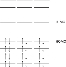
Of all the electron-filled orbitals, the orbital possessing the maximum electron energy is called the highest occupied molecular orbital (HOMO). Conversely, among all the unfilled electron orbitals, the orbital with the lowest electron energy is termed the lowest unoccupied molecular orbital (LUMO). The absolute values of HOMO and LUMO energies relate to the ionization potential and electron affinity (see ). Ionization potential energy is the minimum energy required to extract one electron from the HOMO, and electron affinity is the energy required to add one electron to LUMO so that the system is stabilized [7].
Diagrams showing orientation of highest occupied and lowest unoccupied molecular orbitals (HOMO and LUMO) of typical organic materials.
Before considering the OLED light emission mechanism, it is important for readers to understand the electron configuration in both the ground state and the excited state.
Let us assume that two electrons, 1 and 2, are allocated in different states. Also, let us define  and
and  as Hamiltonians when electrons 1 and 2 exist independently:
 (2.1)
(2.1)
 (2.2)
(2.2)
 (2.3)
(2.3)
Here, H′ is perturbation due to electron repulsion.
When two electrons are allocated in different states, the Hamiltonian can be expressed as follows:
 (2.4)
(2.4)
If there is no perturbation, the solution of the wave equation can be expressed as follows.

Calculus of variation is useful here for solving the equation that accounts for perturbation, as follows:
 (2.6)
(2.6)
Energy E should be the minimum in calculus variation:

As ψA, ψB are orthogonalized and normalized with respect to each other, the equation can be expressed as

Here
 (2.9)
(2.9)
and by applying the orthogonalization condition, we obtain
 (2.10)
Therefore, can be expressed as follows:
 (2.11)
Here, J is the Coulomb integral, and K is the exchange integral, which can be expressed as follows:
 (2.12)
 (2.13)
Using , we obtain
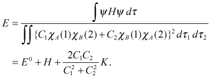
According to the calculus variation method, a condition for ensuring the minimum E value needs to be calculated.
A minimum condition occurs when the value of differentiation of E by C1 and C2 is zero:
 (2.15)
Therefore
 (2.16)
Then
 (2.17)
On the other hand, by applying the normalization condition, we obtain
 (2.18)
Therefore
 (2.19)
Using , we have

Also, by applying , we can obtain the following two wavefunctions:


The spin contribution of the actual molecular system must be considered in addition to the conclusion reached in Section 2.2.2.2 regarding electron configuration.
The wavefunction corresponding to spin quantum number  (spin function) is expressed as α or β.
According to the same reasoning applied in Section 2.2.2.2, the characteristic spin function of a two-electron system can be expressed as follows:
 (2.22)
When spin function is taken into account, the polarity of the wavefunction must change with respect to characteristic function swapping, as indicated in Eqs. and ; the wavefunction can then be expressed as follows:

The degeneration states with respect to three wavefunctions can be expressed as follows:

In total, four states, one in and three in , are formed. represents singlet state and , the triplet state.
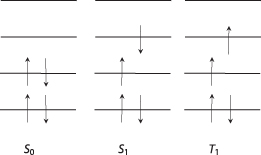
Before excitation, when in the ground state, the electrons are placed with both upward spin and downward spin. When excited, the electron in the upper spin state is allocated with the same spin state (S1), or, for some reason (such as intersystem crossing [ISC]), the spin is reversed (T1) (). The former case is called singlet exciton (a binding state of a pair of excited electrons and hole due to Coulomb force) and the latter triplet exciton; each exciton corresponds to the wavefunctions given in Eqs. and , respectively. Light emission resulting from the energy transfer from singlet state to ground state is termed fluorescence emission; light emission from triplet state to ground state is called phosphorescence emission ().
Electron configurations in ground and excited states.
Emission mechanisms of (a) fluorescence (singlet) and (b) phosphorescence (triplet) (Jablonski energy diagram).

When two electrons are allocated to the same orbital, they form an electron pair with different spin states. This phenomenon is also known as the Pauli exclusion principle, which holds that any two fermions (particles that follow the Fermi–Dirac statistics) of the same type (such as two electrons) cannot occupy the same quantum state simultaneously. Then, the spin direction must be reversed when the electron is changed from the T1 to the S0 state. Usually, this change takes place over a relatively long period of time, so the exciton lifetime (exciton decay time) of the triplet state is relatively longer than that for singlet emission. Also, triplet state T1 is of lower energy than singlet state S1. (This is so because any two electrons of the same spin state cannot approach one another, due to Pauli’s exclusion principle, while two electrons with different spin states can approach each other. As two electrons have the same spin state in triplet, they cannot come closer and result in lower energy than the singlet case.) This phenomenon results in longer wavelength in triplet emission, which often gives rise to invisible light emission (emission at a wavelength longer than the long wavelength extreme of the visible spectrum).