Contents
Cover
Wiley Series in Materials for Electronic and Optoelectronic Applications
Title Page
Copyright
Dedication
In Memoriam: Cole Litton
Series Preface
Preface
List of Contributors
Chapter 1: Fundamental Properties of ZnO
1.1 Introduction
1.2 Band Structure
1.3 Optical Properties
1.4 Electrical Properties
1.5 Band Gap Engineering
1.6 Spintronics
1.7 Summary
References
Chapter 2: Optical Properties of ZnO
2.1 Introduction
2.2 Free Excitons
2.3 Strain Splitting of the Γ5 and Γ6 Free Excitons in ZnO
2.4 Photoluminescence from the Two Polar Faces of ZnO
2.5 Bound-Exciton Complexes in ZnO
2.6 Similarities in the Photoluminescence Mechanisms of ZnO and GaN
2.7 The Combined Effects of Screening and Band Gap Renormalization on the Energy of Optical Transitions in ZnO and GaN
2.8 Closely Spaced Donor–Acceptor Pairs in ZnO
2.9 Summary
References
Chapter 3: Electrical Transport Properties in Zinc Oxide
3.1 Introduction
3.2 Hall-Effect Analysis
3.3 Donor States and n-type Doping
3.4 Hydrogen
3.5 Acceptor States and p-type Doping
3.6 Photoconductivity
3.7 Summary
References
Chapter 4: ZnO Surface Properties and Schottky Contacts
4.1 Historical Background of Schottky Contacts on ZnO
4.2 Recent Schottky Barrier Studies
4.3 The Influence of Surface Preparation on Schottky Barriers
4.4 The Influence of Defects on Schottky Barriers
4.5 The Influence of ZnO Polarity on Schottky Barriers
4.6 The Influence of Chemistry
4.7 Charge Transport and Extended Metal–ZnO Schottky Barriers
4.8 Conclusion
Acknowledgements
References
Chapter 5: Native Point Defects and Doping in ZnO
5.1 Introduction
5.2 Theoretical Framework
5.3 Native Point Defects
5.4 Donor Impurities
5.5 Acceptor Impurities
5.6 Isoelectronic Impurities
Acknowledgements
References
Chapter 6: Spectral Identification of Impurities and Native Defects in ZnO
6.1 Introduction
6.2 Optical Spectroscopy
6.3 Magnetic Resonance Investigations
References
Chapter 7: Vapor Transport Growth of ZnO Substrates and Homoepitaxy of ZnO Device Layers
7.1 Introduction
7.2 Transport Theory and Comparison with Growth Data
7.3 Characterization
7.4 In-situ Doping
7.5 ZnO Homoepitaxy
7.6 Summary
7.7 Acknowledgement
References
Chapter 8: Growth Mechanisms and Properties of Hydrothermal ZnO
8.1 Introduction
8.2 Overview of Hydrothermal Solution Growth
8.3 Thermodynamics of Hydrothermal Growth of ZnO
8.4 Hydrothermal Growth Techniques
8.5 Growth Kinetics of Hydrothermal ZnO
8.6 Properties of Bulk Hydrothermal ZnO
8.7 Conclusion
Acknowledgements
References
Chapter 9: Growth and Characterization of GaN/ZnO Heteroepitaxy and ZnO-Based Hybrid Devices
9.1 Introduction
9.2 Growth of GaN/ZnO
9.3 Compositional Analysis
9.4 Structural Analysis
9.5 Surface Studies
9.6 Optical Properties
9.7 Electrical Properties
9.8 GaN/ZnO Hybrid Devices
9.9 Conclusions
Acknowledgements
References
Chapter 10: Room Temperature Stimulated Emission and ZnO-Based Lasers
10.1 Introduction
10.2 Emission Mechanisms
10.3 Stimulated Emission
10.4 Zinc Oxide Lasers
10.5 Conclusions
References
Chapter 11: ZnO-Based Ultraviolet Detectors
11.1 Introduction
11.2 Photoconductivity in ZnO
11.3 ZnO Film-Based UV Photodetectors
11.4 ZnO NW UV Photodetectors
11.5 Conclusions
Acknowledgements
References
Chapter 12: Room-Temperature Stimulated Emission from ZnO Multiple Quantum Wells Grown on Lattice-Matched Substrates
12.1 Introduction
12.2 Experimental Details
12.3 Quantum Confinement Effect of Excitons in QWs
12.4 Exciton–Phonon Interaction in QWs
12.5 The Localization Mechanism of the Exciton in a QW
12.6 Time-Resolved Luminescence in ZnO QWs
12.7 Stimulated Emission in MQWs
12.8 Summary
Acknowledgements
References
Index
Wiley Series in Materials for Electronic and Optoelectronic Applications
www.wiley.com/go/meoa
Series Editors
Dr Peter Capper, SELEX Galileo Infrared Ltd, Southampton, UK
Professor Safa Kasap, University of Saskatchewan, Canada
Professor Arthur Willoughby, University of Southampton, UK
Published Titles
Bulk Crystal Growth of Electronic, Optical and Optoelectronic Materials, Edited by P. Capper
Properties of Group–IV, III–V and II–VI Semiconductors, S. Adachi
Charge Transport in Disordered Solids with Applications in Electronics, Edited by S. Baranovski
Optical Properties of Condensed Matter and Applications, Edited by J. Singh
Thin Film Solar Cells: Fabrication, Characterization and Applications, Edited by J. Poortmans and V. Arkhipov
Dielectric Films for Advanced Microelectronics, Edited by M. R. Baklanov, M. Green and K. Maex
Liquid Phase Epitaxy of Electronic, Optical and Optoelectronic Materials, Edited by P. Capper and M. Mauk
Molecular Electronics: From Principles to Practice, M. Petty
Luminescent Materials and Applications, Edited by A. Kitai
CVD Diamond for Electronic Devices and Sensors, Edited by R. S. Sussmann
Properties of Semiconductor Alloys: Group–IV, III–V and II–VI Semiconductors, S. Adachi
Mercury Cadmium Telluride: Growth, Properties and Applications, Edited by P. Capper and J. Garland
Forthcoming Titles
Principles of Solar Cells, LEDs and Diodes: The Role of the PN Junction, A. Kitai
Silicon Photonics: Fundamentals and Devices, M. J. Deen and P. K. Basu
Photovoltaic Materials: From Crystalline Silicon to Third–Generation Approaches, Edited by G. J. Conibeer
Inorganic Glasses for Photonics: Fundamentals, Engineering and Applications, A. Jha, R. M. Almeida, M. C. Goncalves and P. G. Kazansky
Lead–Free Solders: Materials Reliability for Electronics, Edited by K.N. Subramanian

Wiley Series in Materials for Electronic and Optoelectronic Applications
www.wiley.com/go/meoa
Series Editors
Dr Peter Capper, SELEX Galileo Infrared Ltd, Southampton, UK
Professor Safa Kasap, University of Saskatchewan, Canada
Professor Arthur Willoughby, University of Southampton, UK
Published Titles
Bulk Crystal Growth of Electronic, Optical and Optoelectronic Materials, Edited by P. Capper
Properties of Group-IV, III–V and II–VI Semiconductors, S. Adachi
Charge Transport in Disordered Solids with Applications in Electronics, Edited by S. Baranovski
Optical Properties of Condensed Matter and Applications, Edited by J. Singh
Thin Film Solar Cells: Fabrication, Characterization and Applications, Edited by J. Poortmans and V. Arkhipov
Dielectric Films for Advanced Microelectronics, Edited by M. R. Baklanov, M. Green and K. Maex
Liquid Phase Epitaxy of Electronic, Optical and Optoelectronic Materials, Edited by P. Capper and M. Mauk
Molecular Electronics: From Principles to Practice, M. Petty
Luminescent Materials and Applications, Edited by A. Kitai
CVD Diamond for Electronic Devices and Sensors, Edited by R. S. Sussmann
Properties of Semiconductor Alloys: Group-IV, III–V and II–VI Semiconductors, S. Adachi
Mercury Cadmium Telluride: Growth, Properties and Applications, Edited by P. Capper and J. Garland
Forthcoming Titles
Principles of Solar Cells, LEDs and Diodes: The Role of the PN Junction, A. Kitai
Silicon Photonics: Fundamentals and Devices, M. J. Deen and P. K. Basu
Photovoltaic Materials: From Crystalline Silicon to Third-Generation Approaches, Edited by G. J. Conibeer
Inorganic Glasses for Photonics: Fundamentals, Engineering and Applications,
A. Jha, R. M. Almeida, M. C. Goncalves and P. G. Kazansky
Lead-Free Solders: Materials Reliability for Electronics, Edited by K.N. Subramanian
This book is dedicated to the memory of Cole W. Litton who was
the driving force behind it and the lead editor. Cole passed
away before its completion.
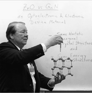
In Memoriam: Cole Litton
Cole W. Litton, the editor and compiler of Zinc Oxide Materials for Electronic and Optoelectronic Device Applications, died of a heart attack on Tuesday, January 26, 2010, while attending the SPIE Photonics West Conference in San Francisco.
Cole was a native of Memphis, Tennessee, born in 1930, and he attended the University of Tennessee graduating with a bachelor's degree. He served for four years as an officer in the US Air Force and then joined the Air Force Research Laboratory as a civilian scientist at Wright Patterson Air Force Base in Dayton, Ohio. There he worked on the solid-state physics team of Don Reynolds, Tom Collins, and later David Look, and was the principal designer of what became the world's highest resolution optical spectrometer. He spent 50 years with the Air Force during which time he studied at several other universities in the United States and Europe. Litton was acknowledged as a world leader in research in solid-state and semiconductor physics and crystal growth, particularly in the optical, electrical, and structural properties of compound semiconductor materials and devices. In 1971 Cole was elected a fellow of the American
Physical Society. He has been a long-time devoted member of SPIE, where he was a founder and current co-chair of the Gallium Nitride Materials and Devices Conference and also the Oxide-Based Materials and Devices Conference, two of the most successful conferences at Photonics West since their inception. In memory of Litton, the Gallium Nitride Materials and Devices Conference will now bear his name, recognizing his many contributions not only to SPIE but to advancing optics- and photonics-based research as well.

Cole Litton retired in 2006 as Senior Scientist from the Air Force Research Laboratory, but he continued to enjoy an active role in scientific workshops and symposia. At the time of his death, he had authored or co-authored about 200 scientific/technical research papers published in physics and engineering journals. He was committed to discovery and was passionate about the future of science and technology. Cole died fully engaged in the activity he most enjoyed: participating in scientific meetings. He was a unique individual with a great love of life, and he will be remembered by all who knew him.
David F. Bliss
US Air Force Laboratory
Hanscom Research Site
MA, USA
Series Preface
WILEY SERIES IN MATERIALS FOR ELECTRONIC AND OPTOELECTRONIC APPLICATIONS
This book series is devoted to the rapidly developing class of materials used for electronic and optoelectronic applications. It is designed to provide much-needed information on the fundamental scientific principles of these materials, together with how these are employed in technological applications. The books are aimed at (postgraduate) students, researchers and technologists, engaged in research, development and the study of materials in electronics and photonics, and industrial scientists developing new materials, devices and circuits for the electronic, optoelectronic and communications industries.
The development of new electronic and optoelectronic materials depends not only on materials engineering at a practical level, but also on a clear understanding of the properties of materials, and the fundamental science behind these properties. It is the properties of a material that eventually determine its usefulness in an application. The series therefore also includes such titles as electrical conduction in solids, optical properties, thermal properties, and so on, all with applications and examples of materials in electronics and optoelectronics. The characterization of materials is also covered within the series in as much as it is impossible to develop new materials without the proper characterization of their structure and properties. Structure–property relationships have always been fundamentally and intrinsically important to materials science and engineering.
Materials science is well known for being one of the most interdisciplinary sciences. It is the interdisciplinary aspect of materials science that has led to many exciting discoveries, new materials and new applications. It is not unusual to find scientists with a chemical engineering background working on materials projects with applications in electronics. In selecting titles for the series, we have tried to maintain the interdisciplinary aspect of the field, and hence its excitement to researchers in this field.
Peter Capper
Safa Kasap
Arthur Willoughby
Preface
Zinc oxide (ZnO) powder has been widely used as a major white paint pigment and industrial processing chemical for nearly 150 years. Indeed, interest in this fascinating chemical compound dates back even to antiquity. ZnO, the first man-made zinc compound, originated many centuries ago as an impure by-product of copper smelting. The ancients discovered and put to use some of its unusual properties, which included production of the first brass metal, development of a purified ZnO for medical purposes, and the early alchemists even attempted to make gold with it. Beginning in the early 1900s, white, polycrystalline ZnO powder found extensive application in medical technology, in particular the cosmetics and pharmaceutical industries, where it is today used in facial and body powders, sun screen preparation, antibiotic lotions and salves and in dental technology for dental cements.
A modern rediscovery of ZnO and its potential applications began in the mid 1950s. At that time, science and industry alike, mostly in the US and Europe, began to realize that ZnO had many interesting novel properties that were worthy of further investigation and exploration. These novel properties included its semiconductor, piezoelectric, luminescent, ultraviolet (UV) absorption, catalytic, ferrite, photoconductive and photochemical properties. Although study of the photoluminescence and electroluminescence properties of ZnO began as early as the mid 1930s, extensive investigation of its semiconductor properties did not begin until the mid to late 1950s, once good single crystals became available, either from natural sources, or grown synthetically by vapor transport and various other techniques, for study of the optical, electrical and structural properties of semiconducting ZnO. These early ZnO single crystals, mostly needles, platelets and prisms, were, however, small and limited in size to a few millimeters. ZnO single crystals typically crystallize in the wurtzitic, hexagonal modification, are visibly transparent and have a wide, direct band gap in the near UV at 3.437 eV (at 2 K). During this same period, the late 1950s to early 1960s, it was also recognized that ZnO had very high piezoelectric coefficients which led to the development of ZnO-based piezoelectric transducers, such as sensitive strain gauges and pressure sensors, a technology which continues today. Throughout the 1960s, extensive investigations of the fundamental semiconductor properties of ZnO were made, including study of its energy band structure, band gaps, excitonic properties, electron and hole effective masses, phonon properties and the electrical transport properties of the intrinsic (undoped) material. At this time (the mid to late 1960s) it was also recognized that ZnO, like the other wide band gap II–VI materials, would be difficult to dope controllably with high concentrations of shallow donor and acceptor impurities in order to demonstrate n- and p-type conductivity and p-n junctions, which would be necessary in order to realize the full potential of ZnO in devices, such as UV diode emitters, detectors and transistors. At that time, modern epitaxial growth and doping techniques, such as molecular beam epitaxy (MBE) and metal organic chemical vapor deposition (MOCVD), had not yet been developed, and p-type doping of both epitaxial films and bulk substrates did not exist; moreover, lack of large, bulk single crystals of ZnO also hampered progress in the development of ZnO-based electronic and optoelectronic devices. Nevertheless, much progress has been made over the past four decades (1970 to present) on the development of ZnO-based transducers, varistors, white-light-emitting cathodoluminescent phosphors (in conjunction with ZnS), optically transparent electrically conducting films, optically pumped lasing, MSM-type UV detectors, based on both ZnO (near UV) and MgZnO/ZnO heterostructures (deeper UV), and surface acoustic wave devices, none of which require the use of p-type ZnO.
Demonstration of the first InGaN/GaN-based, long-lived, room-temperature, continuous wave (CW) blue light-emitting diodes (LEDs) and diode lasers in Japan in the mid 1990s, led several ZnO investigators to consider the possibility of using isomorphic, nearly lattice-matched, c-plane bulk ZnO as a substrate for GaN device epitaxy (∼2% mismatch to GaN), since bulk GaN substrates did not exist, and it was clear that the large threading dislocations resulting from growth of InGaN/GaN laser device structures on lattice mismatched c-plane sapphire (∼14% lattice mismatch) were degrading both the performance and lifetimes of the blue laser diodes, particularly in CW, single mode operation. Earlier a US nitride research group had already demonstrated that GaN device epitaxy could be grown by MBE on small, c-plane ZnO substrates with as much as two to three orders of magnitude reduction in threading dislocation densities within the GaN device epitaxy, in comparison with growth on highly lattice mismatched sapphire substrates. Over the past decade, this achievement led another group to successfully grow and market large (40 mm diameter), high-quality, single-crystal ZnO substrates by vapor transport techniques specifically for this purpose and more recently still another group has also developed large diameter, bulk ZnO substrates by the Pressure-Melt technique for this purpose. Work is presently underway to demonstrate the MBE growth of AlGaN/GaN-based microwave power field-effect transistor (FET) device structures, where the relatively cheap ZnO substrate will be etched away and a high thermal conductivity substrate substituted by wafer bonding techniques to improve heat dissipation from the device.
Over the past decade, a number of groups have proposed that ZnO might be a good optoelectronic device material in its own right, owing to the many similarities between the optical, electrical and structural properties of ZnO and GaN, including their band gaps (3.437 eV for ZnO and 3.50 eV for GaN at 2 K) and their lattice constants. In addition, still others have noted that ZnO has a free exciton binding energy of 60 meV, approximately twice that of GaN, which could lead to highly efficient, ZnO- and MgZnO-based, UV injection lasers (UV laser diodes and detectors) at room temperature, provided that efficient p-doping and good p-n junctions and heterojunctions can be demonstrated in these materials. p-type doping of hetero-epitaxial ZnO on sapphire has been reported by several Japanese and US groups, using N acceptor doping and several different growth techniques, with varying degrees of success, but a major breakthrough was achieved by a US group recently which reported the first MBE growth of homo-epitaxial, N-doped, p-type ZnO on high-resistivity, Li-diffused ZnO substrates. Although the temperature-dependent Hall conductivity of these p-type layers is not yet fully understood, this approach could lead rapidly to p-doping at higher hole mobilities and carrier concentration and to the formation of good p-n junctions, provided that we can achieve a better understanding of both the shallow and deep donor/acceptor compensation mechanisms in ZnO. It is important to address the questions of donor and acceptor impurity incorporation together with the likely formation of native point defect donors and acceptors in ZnO and their possible compensation mechanisms; and look into the question of possible hydrogen donor incorporation in ZnO which must be better understood if rapid progress is to be made in the p-doping of ZnO.
This book comprises some 12 chapters that are written by experts in various aspects of ZnO materials and device technology. The topics included and discussed in these chapters range from our latest understanding of the energy band structure and spintronics (Chapter 1) to our most recent understanding of the fundamental optical and electrical properties of ZnO (Chapters 2 and 3). With the generation of new devices, one has to understand and control the electronic contacts of ZnO. This is covered in Chapter 4. The latest advances in our understanding of the formation of native point defect donors and acceptors in ZnO are discussed and summarized in Chapter 5. The following chapter (Chapter 6) investigates both the intrinsic and extrinsic defects that are found in ZnO. The growth of the ZnO crystals and substrates are discussed in the next three chapters (Chapters 7, 8 and 9) along with hybrid devices, Chapter 10 reports on some recent advances in optically pumped lasing and room temperature stimulated emission from ZnO-based materials. Chapter 11 reviews the progress of UV photodetectors and points out the promise for unique applications such as single-photon detection. The final chapter (Chapter 12) presents a review of optical properties of ZnO quantum wells in which strong stimulation was observed in ZnO/ZnMgO multiple quantum wells from 5 °C to room temperature.
Cole W. Litton
Donald C. Reynolds
Thomas C. Collins
List of Contributors
M. N. Alexander, Air Force Research Laboratory, Hanscom AFB, MA, USA
D. M. Bagnall, University of Southampton, Southampton, UK
Leonard J. Brillson, The Ohio State University, Columbus, OH, USA
M. J. Callahan, Teleos Solar, Hanson, MA, USA and Air Force Research Laboratory, Hanscom AFB, MA, USA
Gene Cantwell, ZN Technology, Inc., Brea, CA, USA
B. Claflin, Wright State University, Dayton, OH, USA
T. C. Collins, Oklahoma State University, Stillwater, OK, USA
Dirk Ehrentraut, Tohoku University, Aoba-ku, Sendai, Japan
R. J. Hauenstein, Oklahoma State University, Stillwater, OK, USA
A. Hoffmann, Technical University Berlin, Berlin, Germany
D. M. Hofmann, Justus Liebig University Giessen, Giessen, Germany
Anderson Janotti, University of California, Santa Barbara, CA, USA
Masashi Kawasaki, Tohoku University, Sendai, Japan, Cross-Correlated Materials Research Group, Advanced Science Institute, RIKEN, Wako, Japan and CREST, Japan Science and Technology Agency, Tokyo, Japan
Hideomi Koinuma, The University of Tokyo, Kashiwa, Chiba, Japan
C. W. Litton, Air Force Research Laboratory, Wright-Patterson Air Force Base, OH, USA
D. C. Look, Wright State University, Dayton, OH, USA
Yicheng Lu, Rutgers University, Piscataway, NJ, USA
Takayuki Makino, Tohoku University, Sendai, Japan
B. K. Meyer, Justus Liebig University Giessen, Giessen, Germany
Hadis Morkoç, Virginia Commonwealth University, Richmond, VA, USA
D. C. Reynolds, Wright State University, Dayton, OH, USA and Air Force Research Laboratory, Wright-Patterson Air Force Base, OH, USA
Yusaburo Segawa, Advanced Science Institute, RIKEN, Wako, Japan
Ryoko Shimada, Virginia Commonwealth University, Richmond, VA, USA
J. J. Song, ZN Technology, Inc., Brea, CA, USA and University of California at San Diego, La Jolla, CA, USA
J. Stehr, Justus Liebig University Giessen, Giessen, Germany
Chris G. Van de Walle, University of California, Santa Barbara, CA, USA
Buguo Wang, Solid State Scientific Inc., Nashua, NH, USA
Jizhi Zhang, ZN Technology, Inc., Brea, CA, USA
Jian Zhong, Rutgers University, Piscataway, NJ, USA
