
Table of Contents
Title Page
Copyright
Dedication
Preface
List of Abbreviations
List of Symbols
Chapter 1: Introduction
1.1 Radiofrequency and Microwave Applications
1.2 Frequency Bands
1.3 Physical Phenomena in the High Frequency Domain
1.4 Outline of the Following Chapters
References
Chapter 2: Electromagnetic Fields and Waves
2.1 Electric and Magnetic Fields
2.2 Maxwell's Equations
2.3 Classification of Electromagnetic Problems
2.4 Skin Effect
2.5 Electromagnetic Waves
2.6 Summary
2.7 Problems
References
Further Reading
Chapter 3: Transmission Line Theory and Transient Signals on Lines
3.1 Transmission Line Theory
3.2 Transient Signals on Transmission Lines
3.3 Eye Diagram
3.4 Summary
3.5 Problems
References
Further Reading
Chapter 4: Transmission Lines and Waveguides
4.1 Overview
4.2 Coaxial Line
4.3 Microstrip Line
4.4 Stripline
4.5 Coplanar Line
4.6 Rectangular Waveguide
4.7 Circular Waveguide
4.8 Two-Wire Line
4.9 Three-Conductor Transmission Line
References
Chapter 5: Scattering Parameters
5.1 Multi-Port Network Representations
5.2 Normalized Power Waves
5.3 Scattering Parameters and Power
5.4 S-Parameter Representation of Network Properties
5.5 Calculation of S-Parameters
5.6 Signal Flow Method
5.7 S-Parameter Measurement
5.8 Problems
References
Further Reading
Chapter 6: RF Components and Circuits
6.1 Equivalent Circuits of Concentrated Passive Components
6.2 Transmission Line Resonator
6.3 Impedance Matching
6.4 Filter
6.5 Transmission Line Filter
6.6 Circulator
6.7 Power Divider
6.8 Branchline Coupler
6.9 Rat Race Coupler
6.10 Directional Coupler
6.11 Balanced-to-Unbalanced Circuits
6.12 Electronic Circuits
6.13 RF Design Software
6.14 Problems
References
Further Reading
Chapter 7: Antennas
7.1 Fundamental Parameters
7.2 Standard Types of Antennas
7.3 Mathematical Treatment of the Hertzian Dipole
7.4 Wire Antennas
7.5 Planar Antennas
7.6 Antenna Arrays
7.7 Modern Antenna Concepts
7.8 Problems
References
Further Reading
Chapter 8: Radio Wave Propagation
8.1 Propagation Mechanisms
8.2 Basic Propagation Models
8.3 Path Loss Models
8.4 Problems
References
Further Reading
Appendix A
A.1 Coordinate Systems
A.2 Logarithmic Representation
Index
First published under the title Hochfrequenztechnik by Carl Hanser Verlag
© Carl Hanser Verlag GmbH & Co. KG, Munich/FRG, 2011
All rights reserved.
Authorized translation from the original German language published by Carl Hanser Verlag GmbH & Co. KG, Munich.FRG.
This edition first published 2012
© 2012 John Wiley & Sons Ltd, Chichester, UK
Registered office
John Wiley & Sons Ltd, The Atrium, Southern Gate, Chichester, West Sussex, PO19 8SQ, United Kingdom
For details of our global editorial offices, for customer services and for information about how to apply for permission to reuse the copyright material in this book please see our website at www.wiley.com.
The right of the author to be identified as the author of this work has been asserted in accordance with the Copyright, Designs and Patents Act 1988.
All rights reserved. No part of this publication may be reproduced, stored in a retrieval system, or transmitted, in any form or by any means, electronic, mechanical, photocopying, recording or otherwise, except as permitted by the UK Copyright, Designs and Patents Act 1988, without the prior permission of the publisher.
MATLAB© is a trademark of The MathWorks, Inc. and is used with permission. The MathWorks does not warrant the accuracy of the text or exercises in this book. This book's use or discussion of MATLAB© software or related products does not constitute endorsement or sponsorship by The MathWorks of a particular pedagogical approach or particular use of the MATLAB© software.
Wiley also publishes its books in a variety of electronic formats. Some content that appears in print may not be available in electronic books.
Designations used by companies to distinguish their products are often claimed as trademarks. All brand names and product names used in this book are trade names, service marks, trademarks or registered trademarks of their respective owners. The publisher is not associated with any product or vendor mentioned in this book. This publication is designed to provide accurate and authoritative information in regard to the subject matter covered. It is sold on the understanding that the publisher is not engaged in rendering professional services. If professional advice or other expert assistance is required, the services of a competent professional should be sought.
Library of Congress Cataloging-in-Publication Data
Gustrau, Frank.
[Hochfrequenztechnik. English]
RF and microwave engineering : fundamentals of wireless communications / Frank Gustrau.
p. cm.
Includes bibliographical references and index.
ISBN 978-1-119-95171-1 (pbk.)
1. Radio circuits. 2. Microwave circuits. 3. Wireless communication systems–Equipment and supplies. I. Title.
TK6560.G8613 2012
621.382–dc23
2012007565
A catalogue record for this book is available from the British Library.
Paper ISBN: 9781119951711
For Sabine, Lisa & Benni
Preface
This textbook aims to provide students with a fundamental and practical understanding of the basic principles of radio frequency and microwave engineering as well as with physical aspects of wireless communications.
In recent years, wireless technology has become increasingly common, especially in the fields of communication (e.g. data networks, mobile telephony), identification (RFID), navigation (GPS) and detection (radar). Ever since, radio applications have been using comparatively high carrier frequencies, which enable better use of the electromagnetic spectrum and allow the design of much more efficient antennas. Based on low-cost manufacturing processes and modern computer aided design tools, new areas of application will enable the use of higher bandwidths in the future.
If we look at circuit technology today, we can see that high-speed digital circuits with their high data rates reach the radio frequency range. Consequently, digital circuit designers face new design challenges: transmission lines need a more refined treatment, parasitic coupling between adjacent components becomes more apparent, resonant structures show unintentional electromagnetic radiation and distributed structures may offer advantages over classical lumped elements. Digital technology will therefore move closer to RF concepts like transmission line theory and electromagnetic field-based design approaches.
Today we can see the use of various radio applications and high-data-rate communication systems in many technical products, for example, those from the automotive sector, which once was solely associated with mechanical engineering. Therefore, the basic principles of radio frequency technology today are no longer just another side discipline, but provide the foundations to various fields of engineering such as electrical engineering, information and communications technology as well as adjoining mechatronics and automotive engineering.
The field of radio frequency and microwave covers a wide range of topics. This full range is, of course, beyond the scope of this textbook that focuses on the fundamentals of the subject. A distinctive feature of high frequency technology compared to classical electrical engineering is the fact that dimensions of structures are no longer small compared to the wavelength. The resulting wave propagation processes then lead to typical high frequency phenomena: reflection, resonance and radiation. Hence, the centre point of attention of this book is wave propagation, its representation, its effects and its utilization in passive circuits and antenna structures.
What I have excluded from this book are active electronic components—like transistors—and the whole spectrum of high frequency electronics, such as the design of amplifiers, mixers and oscillators. In order to deal with this in detail, the basics of electronic circuit design theory and semiconductor physics would be required. Those topics are beyond the scope of this book.
If we look at conceptualizing RF components and antennas today, we can clearly see that software tools for Electronic Design Automation (EDA) have become an essential part of the whole process. Therefore, various design examples have been incorporated with the use of both circuit simulators and electromagnetic (EM) simulation software. The following programs have been applied:
As the market of such software products is ever changing, the readers are highly recommended to start their own research and find the product that best fits their needs.
At the end of each chapter, problems are given in order to deepen the reader's understanding of the chapter material and practice the new competences. Solutions to the problems are being published and updated by the author on the following Internet address:
Finally, and with great pleasure, I would like to say thank you to my colleagues and students who have made helpful suggestions to this book by proofreading passages or initiating invaluable discussions during the course of my lectures. Last but not the least I express gratitude to my family for continuously supporting me all the way from the beginning to the completion of this book.
Frank Gustrau
Dortmund, Germany
List of Abbreviations
| 3GPP | Third Generation Partnership Project |
| Al2O3 | Alumina |
| Balun | Balanced-Unbalanced |
| CAD | Computer Aided Design |
| DC | Direct Current |
| DFT | Discrete Fourier Transform |
| DUT | Device Under Test |
| EM | ElectroMagnetic |
| EMC | ElectroMagnetic Compatibility |
| ESR | Equivalent Series Resistance |
| FDTD | Finite-Difference Time-Domain |
| FEM | Finite Element Method |
| FR4 | Glass reinforced epoxy laminate |
| GaAs | Gallium arsenide |
| GPS | Global Positioning System |
| GSM | Global System for Mobile Communication |
| GTD | Geometrical Theory of Diffraction |
| GUI | Graphical User Interface |
| HPBW | Half Power Beam Width |
| ICNIRP | International Commission on Non-Ionizing Radiation Protection |
| IFA | Inverted-F Antenna |
| ISM | Industrial, Scientific, Medical |
| ITU | International Communications Union |
| LHCP | Left-Hand Circular Polarization |
| LHEP | Left-Hand Elliptical Polarization |
| LNA | Low-Noise Amplifier |
| LOS | Line of Sight |
| LTE | Long Term Evolution |
| LTI | Linear Time-Invariant |
| MIMO | Multiple-Input Multiple-Output |
| MMIC | Monolithic Microwave Integrated Circuits |
| MoM | Method Of Moments |
| NA | Network Analyser |
| NLOS | Non Line of Sight |
| PA | Power Amplifier |
| PCB | Printed Circuit Board |
| PEC | Perfect Electric Conductor |
| PML | Perfectly Matched Layer |
| PTFE | Polytetraflouroethylene |
| Radar | Radio Detection and Ranging |
| RCS | Radar Cross-Section |
| RF | Radio Frequency |
| RFID | Radio Frequency Identification |
| RHCP | Right-Hand Circular Polarization |
| RHEP | Right-Hand Elliptical Polarization |
| RMS | Root Mean Square |
| SAR | Specific Absorption Rate |
| SMA | SubMiniature Type A |
| SMD | Surface Mounted Device |
| TEM | Transversal Electromagnetic |
| UMTS | Universal Mobile Telecommunication System |
| UTD | Uniform Theory of Diffraction |
| UWB | Ultra-WideBand |
| VNA | Vector Network Analyser |
| VSWR | Voltage Standing Wave Ratio |
| WLAN | Wireless Local Area Network |
List of Symbols
Latin Letters
| A | Area (m2) |
| AdB | Attenuation (dB) |
 |
Magnetic vector potential (Tm) |
| Aeff | Effective antenna area (m2) |
| A | ABCD matrix (matrix elements have different units) |
 |
Magnetic flux density (magnetic induction) (T; Tesla) |
| B | Bandwidth (Hz; Hertz) |
| BW | Bandwidth (angular frequency) (1/s) |
| c | Velocity of a wave (m/s) |
| C | Capacitance (F; Farad) |
| C(φ, ϑ) | Radiation pattern function (dimensionless) |
| C′ | Capacitance per unit length (F/m) |
| D | Directivity (dimensionless) |
 |
Electric flux density (C/m2) |
 |
Electric field strength (V/m) |
| f | Frequency (Hz) |
| fc | Cut-off frequency (Hz) |
 |
Force (N; Newton) |
 |
Coulomb Force (N) |
 |
Lorentz Force (N) |
| G | Conductance (1/Ω = S) |
| G | Gain (dimensionless) |
| G | Green's function (1/m) |
| G′ | Conductance per unit length (S/m) |
 |
Magnetic field strength (A/m) |
| H | Hybrid matrix (matrix elements have different units) |
| I | Current (A; Ampere) |
| I | Identity matrix (dimensionless) |
| j | Imaginary unit (dimensionless) |
 |
Electric current density (A/m2) |
 |
Surface current density (A/m) |
| k | Coupling coefficient (dimensionless) |
| k | Wavenumber (1/m) |
| kc | Cut-off wavenumber (1/m) |
 |
Wave vector (1/m) |
 , L , L |
Length (m) |
| L | Inductance (H; Henry) |
| L | Pathloss (dimensionless) |
| L′ | Inductance per unit length (H/m) |
| p | Power density (W/m3) |
| P | Power (W; Watt) |
| Pantenna | Accepted power (W) |
| Pinc | Incoming power (W) |
| Prad | Radiated power (W) |
| Q | Charge (C; Coulomb) |
| Q | Quality factor (dimensionless) |
| r | Radial coordinate (m) |
| R | Resistance (Ω) |
| RDC | Resistance for steady currents (Ω) |
| RESR | Equivalent series resistance (Ω) |
| RRF | Resistance for radio frequencies (Ω) |
| Rrad | Radiation resistance (Ω) |
| R′ | Resistance per unit length (Ω/m) |
| skl | Scattering parameter (dimensionless) |
| S | Scattering matrix (dimensionless) |
 |
Poynting vector (W/m2) |
 |
Average value of Poynting vector (W/m2) |
| t | Time (s; second) |
| T | Period (s) |
| tanδ | Loss tangent (dimensionless) |
| U | Voltage (V; Volt) |
 |
Velocity (m/s) |
| vgr | Group velocity (m/s) |
| vph | Phase velocity (m/s) |
| V | Volume (m3) |
| we | Electric energy density (J/m3) |
| We | Electric energy (J; Joule) |
| wm | Magnetic energy density (J/m3) |
| Wm | Magnetic energy (J) |
| x, y, z | Cartesian coordinates (m) |
| Y | Admittance (S; Siemens) |
| Y | Admittance matrix (S) |
| ZA | Load impedance (Ω) |
| ZF | Characteristic wave impedance (Ω) |
| ZF0 | Characteristic impedance of free space (Ω) |
| Zin | Input impedance (Ω) |
| Z0 | Characteristic line impedance (Ω) |
| Port reference impedance (Ω) | |
| Z0,cm | Common mode line impedance (Ω) |
| Z0,diff | Differential mode line impedance (Ω) |
| Z0e | Even mode line impedance (Ω) |
| Z0o | Odd mode line impedance (Ω) |
| Z | Impedance matrix (Ω) |
Greek Letters
| α | Attenuation coefficient (1/m) |
| β | Phase constant (1/m) |
| δ | Skin depth (m) |
| Δ | Laplace operator (1/m2) |
| ε = ε0εr | Permittivity (As/(Vm)) |
| εr | Relative permittivity (dimensionless) |
| εr,eff | Effective relative permittivity (dimensionless) |
| η | Radiation efficiency (dimensionless) |
| ηtotal | Total radiation efficiency (dimensionless) |
| γ | Propagation constant (1/m) |
| λ | Wavelength (m) |
| λW | Wavelength inside waveguide (m) |
| μ = μ0μr | Permeability (Vs/(Am)) |
| μr | Relative permeability (dimensionless) |
| ∇ | Nabla operator (1/m) |
| φ | Phase angle (rad) |
| φ | Azimuth angle (rad) |
| ϕ | Scalar electric potential (V) |
| φ0 | Initial phase (rad) |
| Ψe | Electric flux (C) |
| Ψm | Magnetic flux (Wb, Weber) (Vs) |
| ρ | Volume charge density (C/m3) |
| ρS | Surface charge density (C/m2) |
| σ | Conductivity (S/m; Siemens/m) |
| σ | Radar cross-section (m2) |
| ϑ | Elevation angle (rad) |
| ϑiB | Brewster angle (rad) |
| ϑic | Critical angle (rad) |
| ω | Angular frequency (1/s) |
Physical Constants
| μ0 | 4π · 10−7 Vs/(Am) | Permeability of free space |
| ε0 | 8.854 · 10−12 As/(Vm) | Permittivity of free space |
| c0 | 2.99792458 · 108 m/s | Speed of light in vacuum |
| e | 1.602 · 10−19 C | Elementary charge |
| ZF0 | 120 π Ω ≈ 377 Ω | Characteristic impedance of free space |
Chapter 1
Introduction
This chapter provides a short overview on widely used microwave and RF applications and the denomination of frequency bands. We will start out with an illustrative case on wave propagation which will introduce fundamental aspects of high frequency technology. Then we will give an overview of the content of the following chapters to facilitate easy orientation and quick navigation to selected issues.
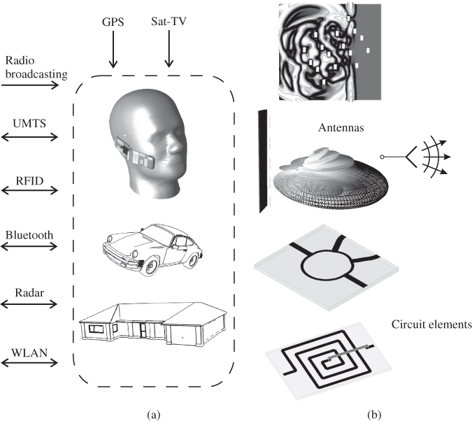
Today, at home or on the move, every one of us uses devices that employ wireless technology to an increasing extent. Figure 1.1 shows a selection of wireless communication, navigation, identification and detection applications.
Figure 1.1 (a) Examples of wireless applications (b) RF components and propagation of electromagnetic waves.
In the future we will see a growing progression of the trend of applying components and systems of high frequency technology to new areas of application. The development and maintenance of such systems requires an extensive knowledge of the high frequency behaviour of basic elements (e.g. resistors, capacitors, inductors, transmission lines, transistors), components (e.g. antennas), circuits (e.g. filters, amplifiers, mixers) including physical issues such as electromagnetic wave propagation.
High frequency technology has always been of major importance in the field of radio applications, recently though RF design methods have started to develop as a crucial factor with rapid digital circuits. Due to the increasing processing speed of digital circuits, high frequency signals occur which, in turn, create demand for RF design methods.
In addition, the high frequency technology's proximity to electromagnetic field theory overlaps with aspects of electromagnetic compatibility (EMC). Setups for conducted and radiated measurements, which are used in this context, are based on principles of high frequency technology. If devices do not comply with EMC limits in general a careful analysis of the circumstances will be required to achieve improvements. Often, high frequency issues play a major role here.
Table 1.1 shows a number of standard RF and microwave applications and their associated frequency bands [1–3]. The applications include terrestrial voice and data communication, that is cellular networks and wireless communication networks, as well as terrestrial and satellite based broadcasting systems. Wireless identification systems (RFID) within ISM bands enjoy increasing popularity among cargo traffic and logistics businesses. As for the field of navigation, GPS should be highlighted, which is already installed in numerous vehicles and mobile devices. Also in the automotive sector, radar systems are used to monitor the surrounding aresa or serve as sensors for driver assistance systems.
Table 1.1 Wireless applications and frequency ranges
| Cellular mobile telephony | ||
| GSM 900 | Global System for Mobile Communication | 880 … 960 MHz |
| GSM 1800 | Global System for Mobile Communication | 1.71 … 1.88 GHz |
| UMTS | Universal Mobile Telecommunications System | 1.92 … 2.17 GHz |
| Tetra | Trunked radio | 440 … 470 MHz |
| Wireless networks | ||
| WLAN | Wireless local area network | 2.45 GHz, 5 GHz |
| Bluetooth | Short range radio | 2.45 GHz |
| Navigation | ||
| GPS | Global Positioning System | 1.2 GHz, 1.575 GHz |
| Identification | ||
| RFID | Radio-Frequency Identification | 13.56 MHz, 868 MHz, |
| 2.45 GHz, 5 GHz | ||
| Radio broadcasting | ||
| FM | Analog broadcast transmitter network | 87.5 … 108 MHz |
| DAB | Digital Audio Broadcasting | 223 … 230 MHz |
| DVB-T | Digital Video Broadcasting - Terrestrial | 470 … 790 MHz |
| DVB-S | Digital Video Broadcasting - Satellite | 10.7 … 12.75 GHz |
| Radar applications | ||
| SRR | Automotive short range radar | 24 GHz |
| ACC | Adaptive cruise control radar | 77 GHz |
For better orientation, the electromagnetic spectrum is divided into a number of frequency bands. Various naming conventions have been established in different parts of the world, which often are used in parallel. Table 1.2 shows a customary classification of the frequency range from 3 Hz to 300 GHz into eight frequency decades according to the recommendation of the International Telecommunications Union (ITU) [4].
Table 1.2 Frequency denomination according to ITU
| Frequency range | Denomination |
| 3 … 30 kHz | VLF - Very Low Frequency |
| 30 … 300 kHz | LF - Low Frequency |
| 300 kHz … 3 MHz | MF - Medium Frequency |
| 3 … 30 MHz | HF - High Frequency |
| 30 … 300 MHz | VHF - Very High Frequency |
| 300 MHz … 3 GHz | UHF - Ultra High Frequency |
| 3 … 30 GHz | SHF - Super High Frequency |
| 30 … 300 GHz | EHF - Extremely High Frequency |
Figure 1.2a shows a commonly used designation of different frequency bands according to IEEE-standards [5]. The unsystematic use of characters and band ranges, which has developed over the years, can be regarded as a clear disadvantage. A more recent naming convention according to NATO is shown by Figure 1.2b [6, 7]. Here, the mapping of characters to frequency bands is much more systematic. However, the band names are not common in practical application yet.
Figure 1.2 Denomination of frequency bands according to different standards. (a) Denomination of frequency bands according to IEEE Std. 521–2002 (b) Denomination of frequency bands according to NATO.

A number of legal foundations and regulative measures ensure fault-free operation of radio applications. Frequency, as a scarce resource, is being divided and carefully administered [8, 9]. Determined frequency bands are allocated to industrial, scientific and medical (ISM) applications. These frequency bands are known as ISM bands and are shown in Table 1.3. As an example, the frequency range at 2.45 GHz is for the operation of microwave ovens and WLAN systems. A further frequency band reserved for wireless non-public short-range data transmission (in Europe) uses the 863 to 870 MHz frequency band [10], for example for RFID applications.
Table 1.3 ISM frequency bands
| 13.553 … 13.567 MHz | 26.957 … 27.283 MHz |
| 40.66 … 40.70 MHz | 433.05 … 434.79 MHz |
| 2.4 … 2.5 GHz | 5.725 … 5.875 GHz |
| 24 … 24.25 GHz | 61 … 61.5 GHz |
| 122 … 123 GHz | 244 … 246 GHz |
We will now take a deeper look at RF engineering through two examples that introduce wave propagation on transmission lines and electromagnetic radiation from antennas.
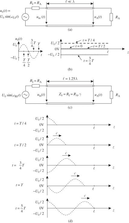
As a first example we consider a simple circuit (Figure 1.3a) with a sinusoidal (monofrequent) voltage source (internal resistance RI), which is connected to a load resistor RA = RI by an electrically short transmission line. Electrically short means that the transmission length  of the line is much shorter than the wavelength λ, that is
 λ. In vacuum–or approximately air–electromagnetic waves propagate with the speed of light c0.
1.1 
Therefore, the free space wavelength λ0 for a frequency f yields:
1.2 
In media other than vacuum the speed of light c is lower and given by
1.3 
where εr is the relative permittivity and μr is the relative permeability of the medium. Typical values for a practical coaxial line would be εr = 2 and μr = 1, resulting in a speed of light of c ≈ 2.12 · 108 m/s on that line. Given–as an example–a frequency of f = 1 MHz we get a wavelength of λ0 = 300 m in free space and λ = 212 m on the previously discussed line. A transmission line of  = 1 m would then be classified as electrically short (
 λ). For simplicity1, we assume further on that the load resistance RA equals the internal resistance RI of the source.
Figure 1.3 Network with voltage source, transmission line and load resistor. Transmission line is electrically short in (a), (b) and electrically long in (c), (d).
Alternatively, electrically short can be expressed by the propagation time τ a signal needs to pass through the entire transmission line. Assuming that electromagnetic processes spread with the speed of light c, the transmission of a signal from the start through to the end of a line requires a time span τ
1.4 
If the time span τ needed for a signal to travel through the whole line is substantially smaller than the cycle time T of its sinusoidal signal, it seems as if the signal change appears simultaneously along the whole line. Signal delay is thus surely negligible.
 is substantially shorter than the wavelength λ of the signal's operating frequency (
 λ) or–in other words–if the duration of a signal travelling from the start to the end of a line τ (delay time) is substantially shorter than its cycle time T (τ
  T).
T).Let us have a look at Figure 1.3b where the current changes slowly in a sinus-like pattern. The term slowly refers to the period T that we assume to be much greater than the propagation time τ along the line. The sine wave starts at t = 0 with a value of zero and reaches its peak after a quarter of the time period (t = T/4). Again after half the time period (t = T/2) it passes through zero and reaches a negative peak at t = 3T/4. This sequence repeats periodically. Since signal delay τ can be omitted compared to the time period T, the signal along the line appears to be spatially constant. According to the voltage divider rule the voltage along the line equals just half of the value of the voltage source u0(t). The input voltage uin(t) and the output (load) voltage uA(t) are–at least approximately–equal.
1.5 
In the next step, we significantly increase the frequency f, so that the line is no longer electrically short. We choose the value of the frequency, such that the line length will equal  = 5/4 · λ = 1.25λ (Figure 1.3c). Now signal delay τ compared to period duration T must be taken into consideration. In Figure 1.3d we can see how far the wave has travelled at times of t = T/4, t = T/2 and so forth. The voltage distribution is no longer spatially constant. After t = 5/4T the signal reaches the end of the line.
Also we can see that the electric voltage uA(t) at the line termination is no longer equal to that at the line input voltage uin(t). A phase difference exists between those two points.
In our example we used a characteristic line impedance Z0 equal to the load and source resistance (Z0 = RA = RI). This is the most simple case and is often applied when using transmission lines. However, if the characteristic line impedance Z0 and terminating resistor RA are not equal to each other, the wave will be reflected at the end of the line. Relationships resulting from these effects will be looked at in Chapter 3 which deals in detail with transmission line theory.
Now let us take a look at a second example. Here we have a geometrically simple structure (Figure 1.4a), which consists of a rectangular metallic patch with side length  arranged above a continuous metallic ground plane. Insulation material (dielectric material) is located between both metallic surfaces. Two terminals are connected to feed the structure.
Figure 1.4 Electrical characteristic of a geometrical simple structure: (a) geometry and (b) imaginary part of admittance.
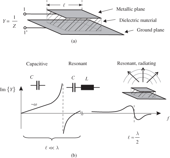
The geometric structure resembles that of a parallel plate capacitor, which has a homogeneous electrical field set up between the metal surfaces. Therefore, we see capacitive behaviour ((Figure 1.4b) Admittance Y = jωC) at low frequency values (geometrical dimensions are significantly below wavelength (
 λ)). By further increasing the frequency, we can observe resonant behaviour due to the unavoidable inductance of feed lines.
At high frequency levels a completely new phenomenon can be observed: with the structure's side length approaching half of a wavelength ( ≈ λ/2), electromagnetic energy will be radiated into space. Now the structure can be used as an antenna (patch antenna).
The last two examples have given us some insight into the fact that problems involving RF cannot simply be treated with conventional methods, but need a toolset adjusted to the characteristics of RF technology. Chapters 2 to 8 therefore give an in-depth insight into how best to solve RF-problems and show the methods we commonly apply.
First, the principles of electromagnetic field theory and wave propagation are reviewed in Chapter 2, in order to understand the mechanisms of passive high-frequency circuits and antennas. The mathematical formulas used in this chapter mainly serve the purpose of illustrating mathematical derivations and are not intended for further calculations. Nowadays, in work practice, modern RF circuit and field simulation software packages provide approximate solutions based on the above mentioned theories. Nonetheless, an engineer needs to understand these mathematical foundations in order to evaluate such given solutions of different commercial software products with respect to their plausibility and accuracy.
Transmission lines are a major and important component in RF circuits. The simple structure of a transmission line may be used in a variety of very different applications. Chapter 3 will therefore deal with the detailed relationships of voltage and current waves on transmission lines. Calculations in this context can be easily followed and form a safe foundation for treating the ever-occurring issue of transmission lines. This chapter gives a short introduction to the Smith chart as a common instrument of presentation and design in RF technology.
Chapter 4 continues with the characterization of transmission line structures and provides a deeper insight into technically important line types such as coaxial lines, planar transmission lines and hollow waveguide structures. It also gives an overview on common mode and differential mode signals on three conductor lines, since they play a major role in the circuit design of filters and couplers.
Chapter 5 introduces scattering parameters, with which the behaviour of RF circuits is characterized. Scattering parameters link wave quantities at different ports of RF circuits. A great advantage of scattering parameters compared to impedance and admittance parameters (which are preferably used when frequency levels are low) is that they can be directly measured by vector network analysers even at high frequencies.
The basic principles provided in Chapters 2 to 5 now pave the way for the description of more complex practical passive RF circuitry, which is the focus of Chapter 6. It is shown that a thoughtful interconnection of transmission lines may create matching circuits, filters, power splitters or couplers. The aim here is to get to know different important design methods and to apply them to examples and case studies, rather than focusing on their mathematical derivation. The examples given are processed with RF circuit and field simulators and thus show how to employ these tools. Also, as a side issue (as it is not the main purpose of this book), a short preview on electronic circuits and their basic characteristics is given.
In radio communication, an antenna provides the link between aerial radio waves in free space and signals on transmission lines. Therefore, Chapter 7 deals with technically important parameters, which serve to describe the radiation behaviour of antennas. To deepen knowledge, we will mathematically deduce the functioning of a basic antenna element (Hertzian dipole). Further on, we take a look at important practical single and array antenna structures and test various design rules on some illustrative examples.
Finally, when it comes to evaluating wireless systems, it is not enough to only consider the antenna alone. Instead, interference from the surroundings (environment) on the wave propagation between antennas must also be taken into account. Chapter 8 thus introduces basic propagation phenomena and their effects on signal transmission. The book concludes with a short review of empirical and physical path loss models.
1. Dobkin DM (2005) RF Engineering for Wireless Networks. Newnes.
2. Golio M, Golio J (2008) The RF and Microwave Handbook, Second Edition. CRC Press.
3. Molisch AF (2011) Wireless Communications. John Wiley & Sons.
4. ITU (2000) ITU-R Recommendation V.431: Nomenclature of the Frequency and Wavelength Bands Used in Telecommunications. International Telecommunication Union.
5. IEEE (2002) IEEE Std 521-2002 Standard Letter Designations for Radar-Frequency Bands. IEEE.
6. Macnamara T (2010) Introduction to Antenna Placement and Installation. John Wiley & Sons.
7. Meinke H, Gundlach FW (1992) Taschenbuch der Hochfrequenztechnik. Springer.
8. Bundesnetzagentur (2008) Frequenznutzungsplan gemaess §54 TKG ueber die Aufteilung des Frequenzbereichs von 9 kHz bis 275 GHz auf die Frequenznutzungen sowie ueber die Festlegungen fuer diese Frequenznutzungen. Bundesnetzagentur.
9. CEPT/ECC (2009) The European Table of Frequency Allocations and Utilizations in the frequency range 9 kHz to 3000 GHz. European Conference of Postal and Telecommunications Administrations, Electronic Communications Committee.
10. Bundesnetzagentur (2005) Allgemeinzuteilung von Frequenzen fuer nichtoeffentliche Funkanwendungen geringer Reichweite zur Datenuebertragung; Non-specific Short Range Devices (SRD). Bundesnetzagentur Vfg 92.
1 The reason for this determination will become clear when we discuss the fundamentals of transmission line theory in Chapter 3.
Chapter 2
Electromagnetic Fields and Waves
In this chapter we will recall the basic electric and magnetic field quantities. We start with the static—non time-varying—case and highlight the relation between electromagnetic field quantities and circuit variables like voltage and current. A full description of time-varying electromagnetic fields is given by Maxwell's equations in combination with additional boundary conditions. Finally we discuss important solutions of Maxwell's equations that are necessary for the understanding of high-frequency behaviour of technical components like transmission lines and antennas.
Our discussion on electromagnetic theory is limited to fundamental aspects. More detailed treatments on this topic can be found in [1–6].
In this section we introduce mathematical formulas and physical relations for the static case in order to get a visual understanding of electric and magnetic field quantities.
Historically it has been known for a long time that electric charges are the origin of electrical phenomena. Charges produce forces upon each other. We distinguish between positive and negative charges. Charges of opposite signs attract each other whereas charges of same sign push each other away. The absolute value of the Coulomb force FC between two point charges1 Q1 and Q2, separated by a distance r, is given by
2.1 
where ε0 = 8.854 · 10−12 As/(Vm) is the permittivity of free space.
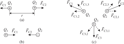
The direction of the Coulomb force is defined by a straight line through both charges (see Figure 2.1a and 2.1b). In the case of three or more charges we can add up the vectors of the forces by the principle of superposition (vector sum in Figure 2.1c).
Figure 2.1 Coulomb forces between (a) two positive charges, (b) two charges of opposite polarity and (c) three charges of equal polarity.
Charges exist in discrete values (integer values of elementary charge e = 1.602 · 10−19 C). However, in practical (macroscopic) engineering configurations the number of charges is so huge that we can treat charge as a continuous quantity.
The abovementioned point-charges are assumed to be located at a single point in space. In the case of a continuous distribution of charges in space we introduce a new term called electric charge density  . The total charge Q in a certain volume V is then expressed as
2.2 
Now we will replace the concept of direct forces between distant charges by a new concept of an electric field that emanates from a charge and leads to interaction with other charges. We look at the electric field strength  of charge Q1 at the point in space where a charge Q2 is located. Let us assume a small positive test charge Q2. The electric field
  is given by the force
  upon the test charge Q2 divided by the test charge Q2 itself. Hence, E1 becomes independent of Q2.
2.3 
The vector of the electric field strength  points in the direction of the force
  . Mathematically the electric field is simply the ratio of
  and Q2. Interestingly we can interpret
  as a vector field that exists in the space surrounding charge Q1, even if no test charge Q2 is present. We can easily measure the electric field distribution of charge Q1 by moving a test charge Q2 around charge Q1.
The distribution of the electric vector field of a positive charge Q1—located at the origin of a spherical coordinate system—is directly derived from Coulomb's law in Equation 2.1 as
2.4 
A vector field is conveniently visualized by field lines. Figure 2.2 shows field line representations of different charge configurations. Field lines represent direction and amplitude of the vector fields. The direction of the vector field is oriented tangentially to the field lines, and the density of field lines is a measure of the absolute value (denser field lines meaning higher field amplitude).
Figure 2.2 Electric field lines for (a) a positive point charge, (b) between two positive charges, (c) between two charges of opposite polarity and (d) in a parallel-plate capacitor (with fringing fields at the edges).
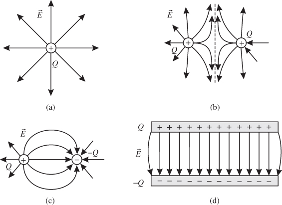
Looking at the field distributions in Figure 2.2 we notice that the electric field lines always2 start at positive charges and end at negative ones. If only positive or negative charges are present the field lines extend to infinity. Therefore, we consider a positive charge as a source of the electric field and a negative charge as a sink.
Consider a charge Q2 that moves through the electric field  of a stationary charge Q1 from point
  to
to  . During movement along the path from
  to
to  the charge Q2 experiences a force
  . From physics we know that work
  is done.
2.5 
The dot product between force  and differential path vector
  indicates that work is maximum for a path tangential to the field lines. A path perpendicular to the force yields zero work. In Equation 2.5 the constant charge Q2 can be taken outside the integral sign. We interpret the integral over the electric field strength as a new electric quantity called voltage U.
2.6 
 . The voltage U is defined between two points
  and
and  and therefore it is an integral or circuit quantity. The voltage is no field quantity.
If we define point  as a fixed reference point
  we derive a new field quantity very similar to the voltage. The electric potential ϕ is given by
2.7 
The electric potential is a scalar field, that is, for any point in space  is given by a single (scalar) value. In the electrostatic case the electric potential ϕ represents the electric voltage between the point
  and the reference point
  .
.
As discussed earlier the electrostatic field  is a conservative field. From mathematics we know that conservative fields can be expressed as a gradient3 of a scalar field. Interestingly the scalar field that leads to the electric field is the negative value of the electric potential
2.8 
Equation 2.8 shows the definition of the gradient operator in Cartesian coordinates. Definitions of the gradient operator in other coordinate systems are listed in Appendix A.1.
The gradient operator on the scalar electric potential results in an electric vector field. The gradient points in the direction of maximum (positive) change in the scalar potential function. The gradient is normal to an equipotential surface (i.e. surface with constant potential). This feature of the gradient is useful when optimization algorithms are considered: in order to find a local maximum of a function it is most efficient to proceed in the direction of maximum change.
The definition of the potential ϕ in Equation 2.7 is ambiguous. There is an infinite number of potential functions since the position of the reference point is not uniquely defined. However the electric field—defined by a force on a charge—is unique. Potentials with different reference points only differ in an additive constant. In Equation 2.8 we see that the electric field is calculated from partial derivatives of the scalar potential. Hence, an additional constant has no impact on the resulting value.
Up to now we have considered charges in free space. In the presence of non-conducting, dielectric materials new expressions can be conveniently defined.
Let us look at a parallel-plate capacitor. The capacitor consists of two ideally conducting plates and a separating dielectric material. In Figure 2.3a the capacitor is filled with vacuum. The charges on both plates are equal in magnitude but have opposite signs: Q+ on the upper plate and Q− on the lower plate. If we assume the lateral extensions of the plates are much larger than the spacing between them we can neglect the fringing fields at the edges and regard the electric field as homogeneous. For the air-filled parallel-plate capacitor in Figure 2.3a we can easily calculate the voltage between the plates from Equation 2.6 as U0 = E0d, where d is the distance between the plates. If we now put an isolating material (dielectric) between the plates (Figure 2.3b), we observe that the new voltage UM is reduced UM < U0. If we remove the dielectric medium the former voltage U0 is restored. The process is reversible.
Figure 2.3 Understanding polarization in a dielectric medium: (a) air-filled parallel-plate capacitor with initial electric field E0, (b) dielectric medium between plates gives rise to an opposing field EP (c) reduced electric field strength EM inside the dielectric medium, (d) dipoles in random order without external electric field and (e) dipoles aligned by external field.
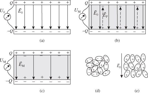
In order to understand the macroscopic effect of reduced voltage when a dielectric is placed inside the capacitor, we will now take a look at the microscopic composition of dielectric materials. We first consider a material that consists of polar particles, that is the molecules represent electric dipoles (Figure 2.3d). Without the external field the dipoles are in random order. Adjacent charges cancel each other out. There is no macroscopic net effect.
If we switch on the external field E0 the dipoles align with the field due to Coulomb forces (Figure 2.3e). In the inner part of the material adjacent charges cancel out. However, at the upper and lower surface of the dielectric material a charge density remains. The surface charge density gives rise to a secondary field EP that is opposed to the external field. Inside the material we observe a diminished field EM
2.9 
This effect is known as polarization.4 The amplitude of polarization, that is the strength of the opposing field EP depends on the microscopic structure of the material.
We have shown that materials with molecules that form electric dipoles can be polarized, that is the dipoles align with the field. It can be shown that even materials with non-dipole molecules can be polarized. Let us consider a simple model of a charge-neutral atom with a positive nucleus in the centre and surrounding negative electrons. The centre of the positive and negative charges is now located at the same point in space. If we put such a material into an external electric field E0 the field exerts opposing forces upon positive and negative charges. This results in a displacement of the charges and induces a dipole moment. Hence we observe a polarizing effect too.
Let us go back now to our initial experiment where a dielectric medium inside the parallel-plate capacitor led to a reduced voltage UM
2.10 
In order to get rid of the description of microscopic effects we focus on the net macroscopic effect: the dielectric material reduces the voltage that we measure and this is as a result of the reduced field EM in the medium. Therefore, we introduce a new term denoted as relative permittivity: the relative permittivity εr is the ratio between the unperturbed external field E0 and the reduced field EM due to polarization
2.11 
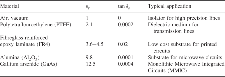
The relative permittivity is a dimensionless quantity equal to or larger than one. Table 2.1 lists values for common engineering materials. Vacuum has a relative permittivity of one, for air the value is slightly higher (εr = 1.0006) [3] but can be considered to be one for nearly all engineering applications.
Table 2.1 Relative permittivity εr and loss tangent tanδε of common dielectric materials in their typical frequency range
There are materials with anisotropic properties, that is the relative permittivity that we measure with our parallel-plate capacitor configuration depends on the orientation of the dielectric material in the capacitor. In this case we can describe the polarizing effect by a matrix rather than by a single value. In this book we will limit our discussion to isotropic materials.
We will close our discussion of microscopic phenomena by looking at time-varying fields. Let us connect our parallel-plate capacitor to a harmonic voltage source. The charges now switch polarity periodically. The dipoles of the dielectric material change their orientation with the same frequency as the field. Above a certain frequency the dipoles cannot follow the external field due to their inertia and the effect of polarization is reduced. Therefore, we expect a decrease of the relative permittivity with frequency.
A model for the frequency dependence εr(f) is given by Debye formulas where f is the frequency of the external field. A detailed discussion is beyond the scope of this text and can be found elsewhere [13]. Fortunately most RF engineering materials have nearly constant relative permittivity values in their technical frequency range of usage.
Another important effect that occurs when a time-varying field is applied is heating of the material. On a microscopic scale the molecules constantly align with the changing field and their movement produces thermal energy (polarization losses). We will see in Section 2.2.4 that this heat loss can be described macroscopically by a term denoted loss tangent. For the purpose of reference we include the loss tangent for important materials in Table 2.1 [8, 9].
Using the permittivity and the electric field strength we define the electric flux density  as a new vector. The letter D comes from the alternate notation of the electric flux density which is displacement.
2.12 
For isotropic materials (εr is a scalar) the electric flux density  and the electric field strength
  are proportional and point in the same direction. The displacement
  is an important vector, as we will see when we discuss Gauss' law in Section 2.2. The unit of
  is C/m2 (Charge per area). Integrating the electric flux density
  over an area A gives us the electric flux Ψe
2.13 
Energy is a common and general concept in physics. In an electric field distribution energy can be stored. The electrostatic energy density is defined as
2.14 
where  is the electric flux density and
  the electric field strength. The latter term in Equation 2.14 is valid for isotropic materials and most convenient for calculations later in this book. The unit of the energy density is Joule/m3.
If we integrate the energy density over a volume V we get the electric energy stored in that volume.
2.15 
Let us assume that the electric field is created by a capacitor with a capacitance C and a voltage U between its electrodes. In this case the energy can be written by using voltage and capacitance as
2.16 
where the volume V includes the complete field between the electrodes.
Capacitance in general is defined as the ratio between charge on the electrodes and voltage between them.
2.17 
For a parallel-plate capacitor with plate area A, plate distance d and dielectric material (relative permittivity εr) between the electrodes the capacitance is
2.18 
In the previous sections we discussed electrostatic fields, that is stationary fields from non-moving charges. Now we consider charges that move in space. We will see that moving charges give rise to magnetic fields.
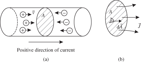
Let us first introduce some useful terms for the description of moving charges. In Figure 2.4a we observe charges ΔQ that move through an area A for a given time interval Δt. The current I then gives the amount of charge ΔQ per time interval Δt.
2.19 
Current—like voltage—is an integrated quantity (not a field quantity), because it depends on an area of observation.
Figure 2.4 (a) Conduction current I as a result of charges passing through a cross-section area A and (b) current density  .
.
AFigure 2.4